Micro/Nanofabrication Center
Physical Vapor Deposition (PVD) of Thin Films One-Day Short Course
Tuesday, 11/12/2024Bowen Hall, Princeton University The Micro/Nano Fabrication Center (MNFC) and Angstrom Engineering are excited to offer a one-day short course on Tuesday, November 12th, 2024, covering Physical Vapor Deposition (PVD) of Thin Films.
The topics covered will include:
- Introduction to Vacuum Science
- Basics of Evaporation and Sputtering Processes
- Mechanical, Electrical, and Optical Properties of Thin Films
- Process Parameters that Affect Film Properties
- Advanced Deposition Troubleshooting
Event Registration
Join us on a virtual tour of the MNFC.
A sampling of the types of research utilizing the MNFC:
PMI MNFC Research Report, 2023PMI MNFC Research Report, 2022
PMI MNFC Research Report, 2019
PMI MNFC Research Report, 2018
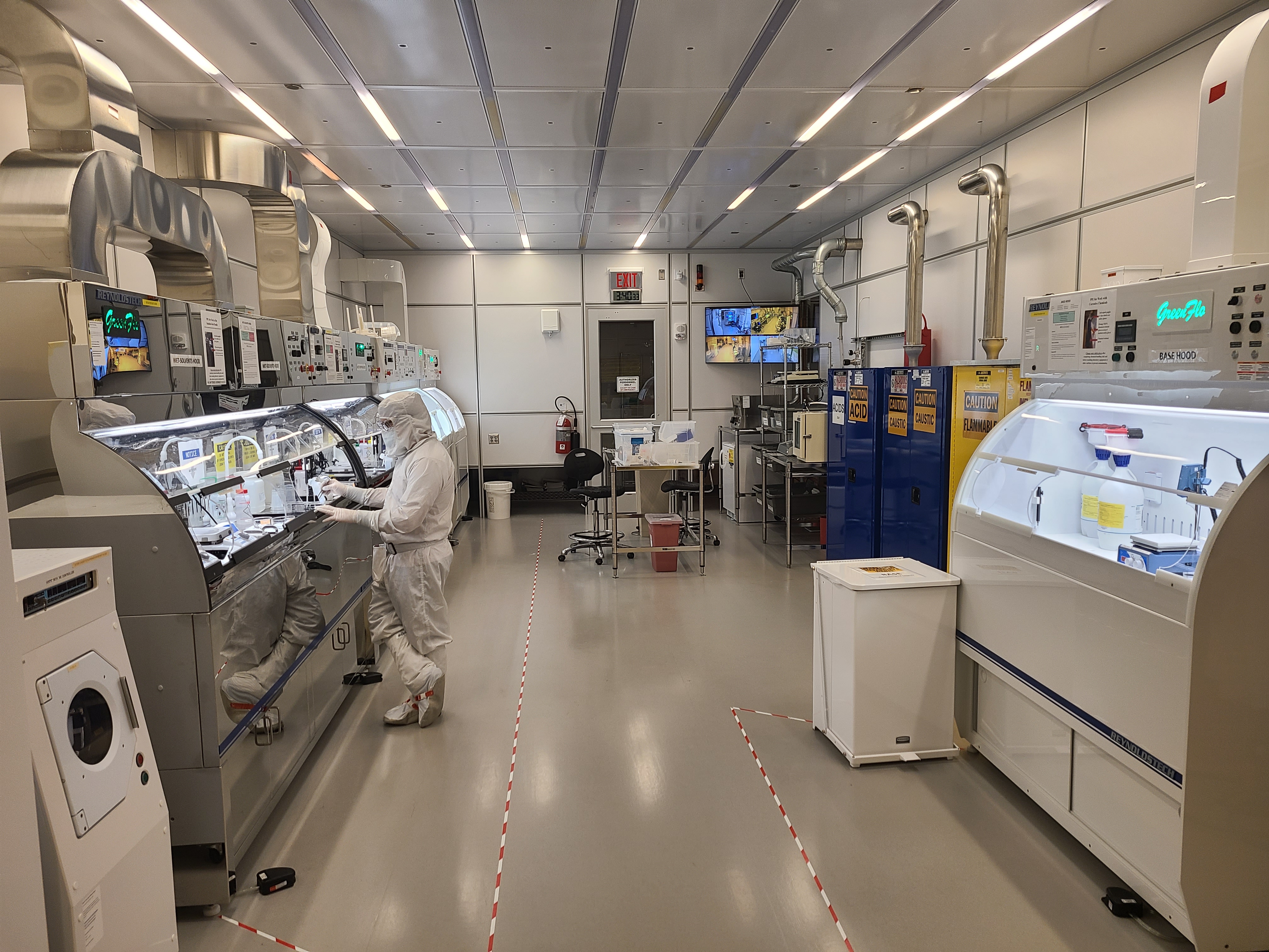
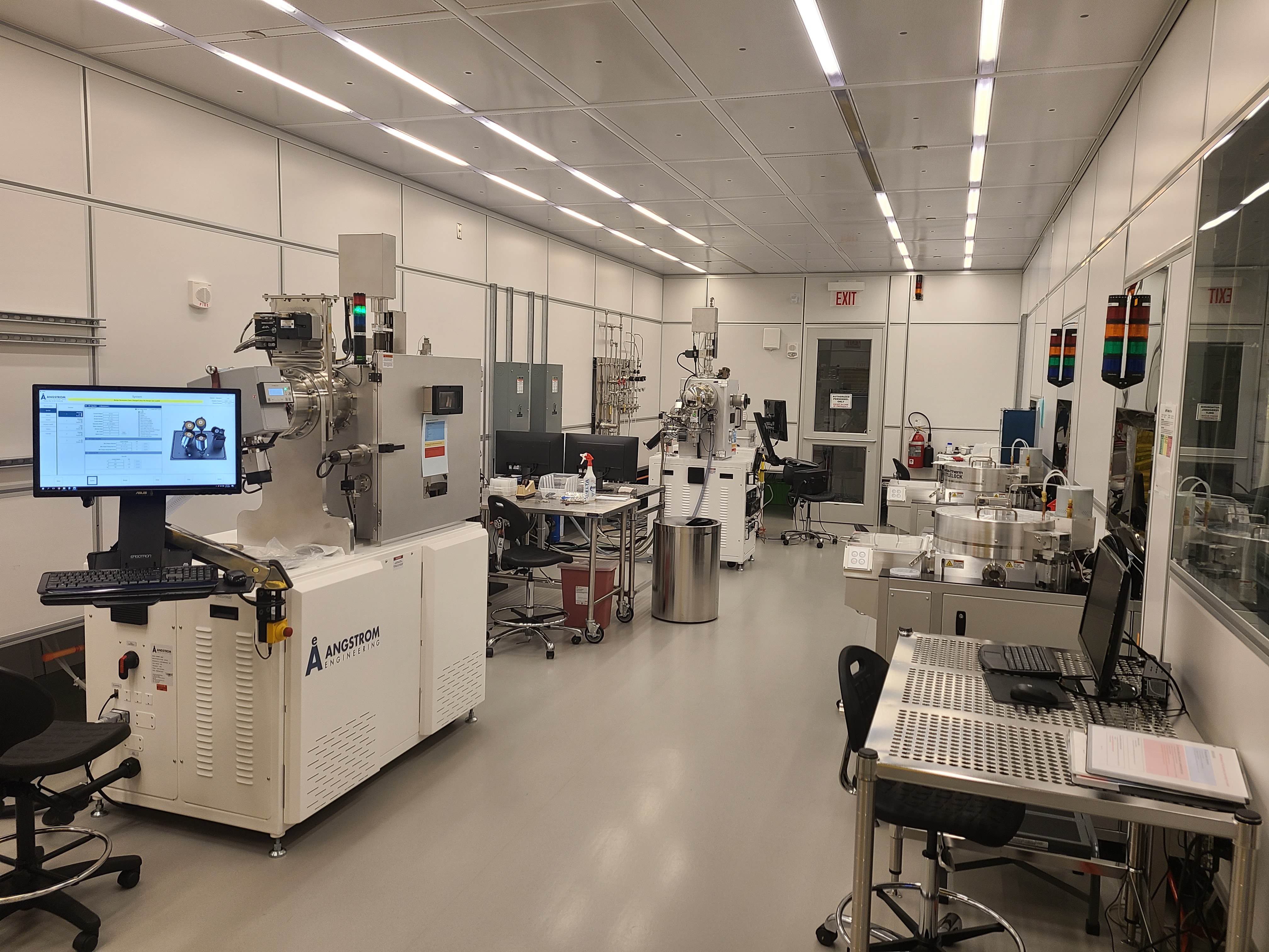
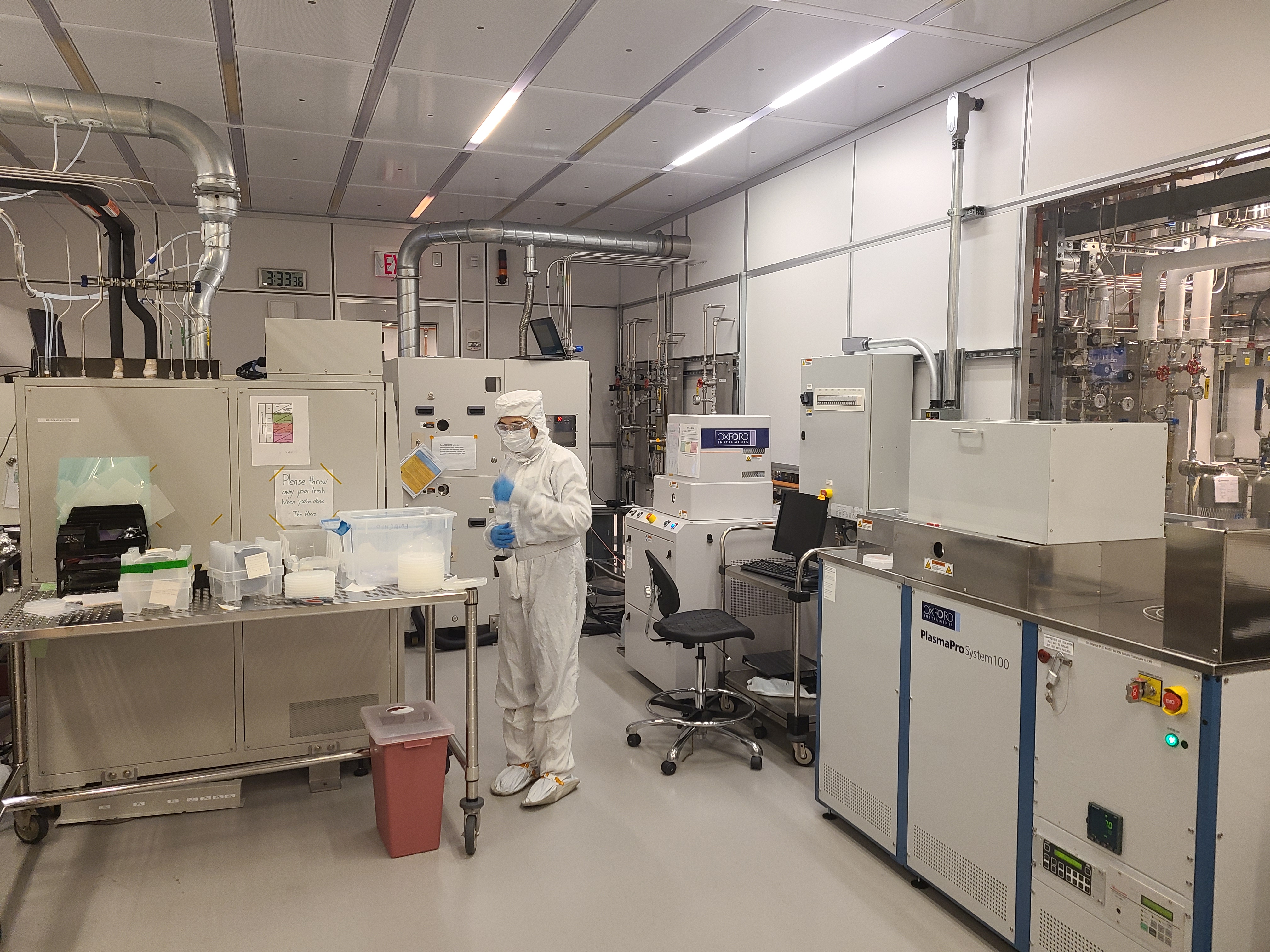
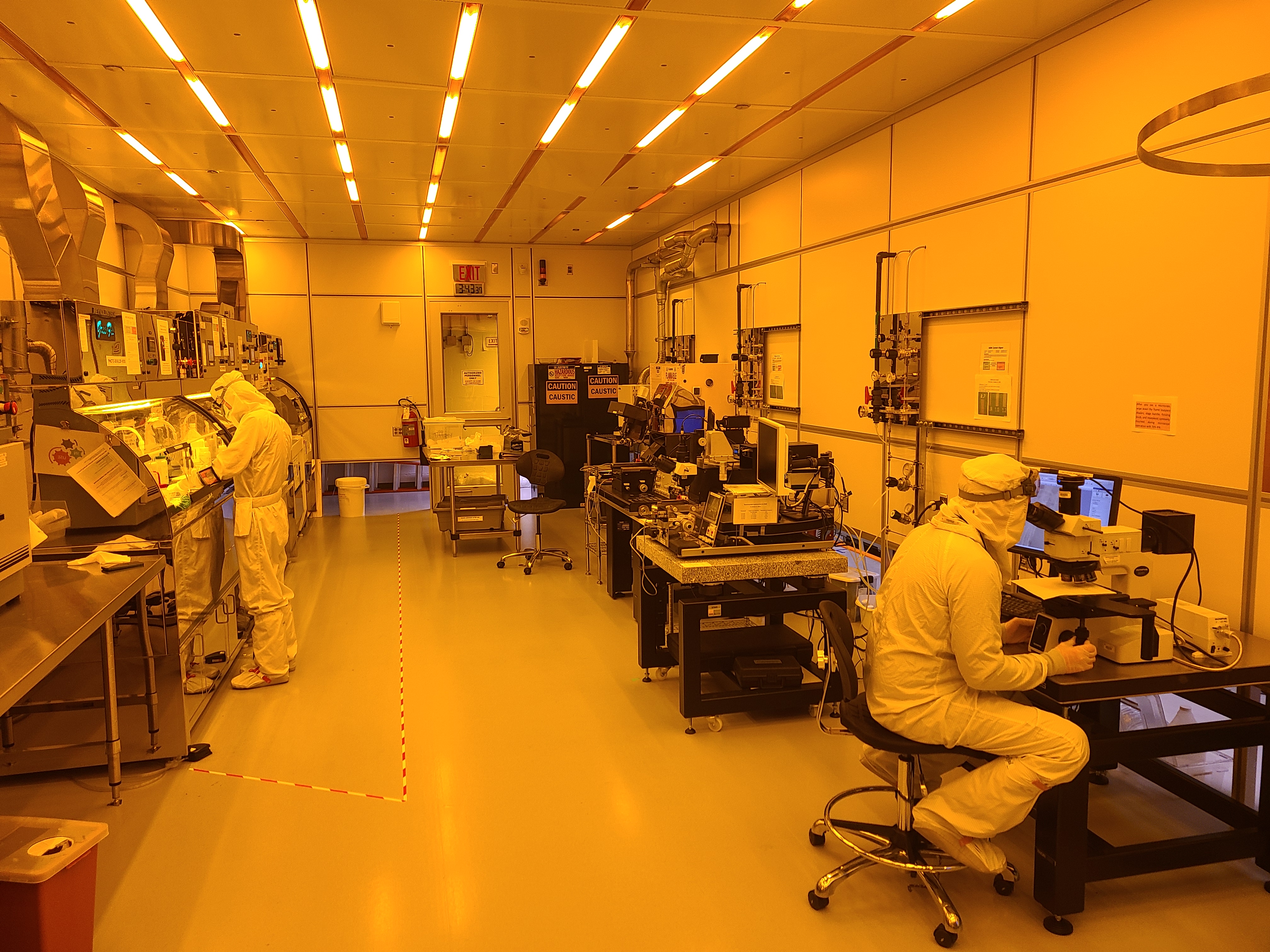
The Princeton Materials Institute created a state-of-the-art cleanroom nanotech fabrication shared research facility used by about 200 students, faculty, research staff, and industrial partners per year. Labmembers use thin film deposition and micro/nano lithographic patterning techniques with a variety of substrates to fabricate devices and structures for electronic, photonic, Micro Electro Mechanical System (MEMS) and biological applications.
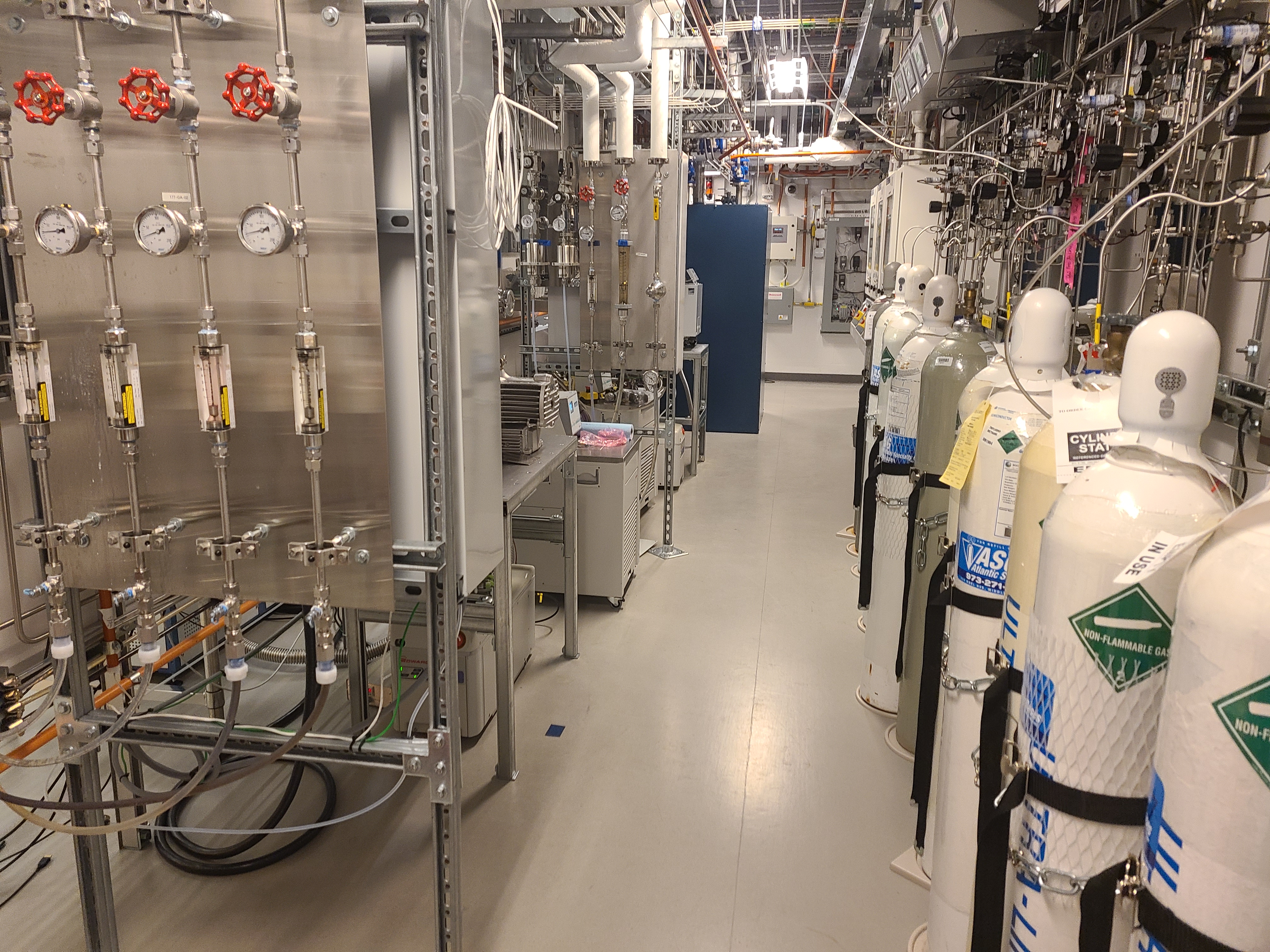
The MNFC with its Soft Materials Processing and Packaging Labs operate in the 129,000 square foot Andlinger Building. The bay/chase cleanroom space occupies two levels of the building and encompasses over 15,000 sq. ft. of C100-C10,000 (ISO 5-7) space using a pressurized plenum design. Contiguous with the main cleanroom is a 1,500 sq. ft. undergraduate teaching lab committed to educating and training. Cornerstone undergraduate courses and lab sessions are taught in this facility.
The Soft Materials (microfluidics) Lab has an independent gowning entrance to prevent cross-contamination into the primary cleanroom. Its capabilities include SU-8 and PDMS processing, a Heidelberg µPG laser direct patterning tool, Form Labs Form 2 3D printers, Nanoscribe Photonic Professional GT2 printer, and PDS 2010 Parylene Coater. These tools and our supporting expertise enable interdisciplinary research and collaborations.
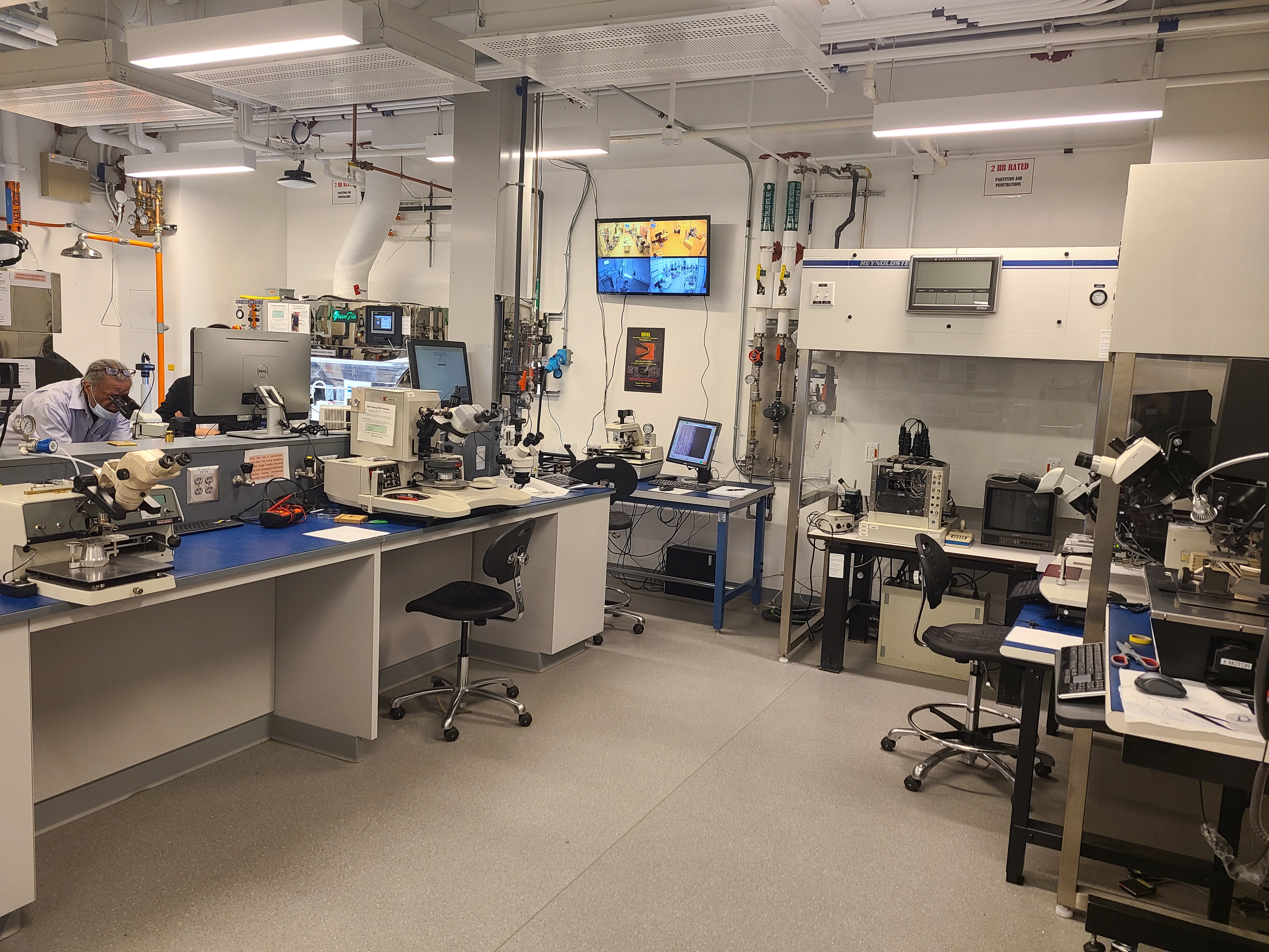
An adjacent stand-alone Packaging Lab is located on the lower level of the building housing a full range of services including dicing & singulation, lapping and polishing, wedge, ball and flip-chip bonding techniques.
MNFC, with its Packaging and Soft Materials Labs together house a broadly encompassing suite of fabrication and characterization tools and associated processes. The tooling and processing set have been established to enable the user base:
- The ability to handle a wide range of substrates: from the usual silicon and III-V semiconductors, to sapphire, glass; as well as plastic and metal foils to support flexible electronics.
- To process a wide range of sample sizes: under 5 mm x 5 mm up to 100 mm wafers (some tools can handle also 150 mm wafers).
- Dry etching and pattern transfer: tools for Si, III-V's, metals, dielectrics, and other materials, in both shallow and deep anisotropic capability.
- Optical lithography: Heidelberg DWL-66+ with greyscale and backside alignment direct laser patterning as well as a standard suite of contact mask aligners.
- Software tools for mask design LEdit, and AutoCAD.
- Nanopatterning: nanoimprint and direct write e-beam lithography, on either piece parts or whole wafers.
- Lapping, polishing, bonding, dicing: a wide range of tools for electrical, optical, and mechanical packaging.
- Multidisciplinary microfluidics to address fluid separation and mixing in physical and life science applications.
MNFC Personnel
Director: Daniel WoodieAssociate Director; PECVD & ALD Process Engineering: Dr. Zuzanna Lewicka
Operations Manager; PVD Process Engineering: Joseph Palmer
Photolithography, Plasma Etch, and Soft Systems: Roman Akhmechet
MNFC Infrastructure and Materials Specialist: Paul Cole
Equipment Engineering: Brien Ely
Backend and Package Engineering: Bert Harrop
 Lab.jpg)
